
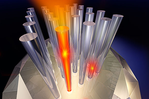
Illustration by Jay Penni
Science & Tech
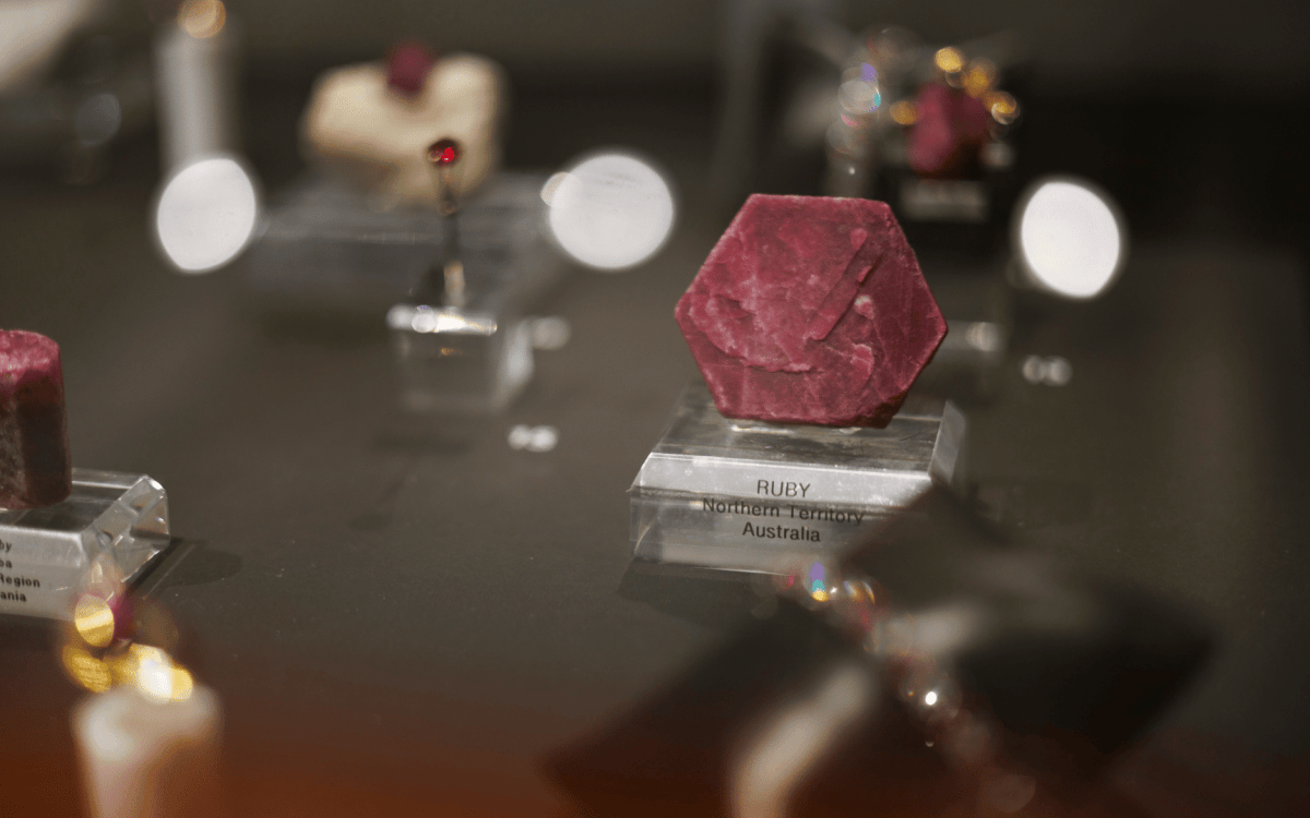
Digging deep into diamonds
Diamond-based nanowire devices advance quantum science
By creating diamond-based nanowire devices, a team at Harvard University has taken another step toward making applications based on quantum science and technology possible.
The new device offers a bright, stable source of single photons at room temperature, an essential element in making fast and secure computing with light practical.
The finding could lead to a new class of nanostructured diamond devices suitable for quantum communication and computing, as well as advance areas ranging from biological and chemical sensing to scientific imaging.
Published in the Feb. 14 issue of Nature Nanotechnology, researchers led by Marko Loncar, assistant professor of electrical engineering at Harvard’s School of Engineering and Applied Sciences (SEAS), found that the performance of a single photon source based on a light-emitting defect (color center) in a diamond could be improved by nanostructuring the diamond and embedding the defect within a diamond nanowire.
Scientists, in fact, first began exploiting the properties of natural diamonds after learning how to manipulate the electron spin, or intrinsic angular momentum, associated with the nitrogen vacancy (NV) color center of the gem. The quantum (qubit) state can be initialized and measured using light.
The color center “communicates” by emitting and absorbing photons. The flow of photons emitted from the color center provides a means to carry the resulting information, making the control, capture, and storage of photons essential for any kind of practical communication or computation. Gathering photons efficiently, however, is difficult since color centers are embedded deep inside the diamond.
“This presents a major problem if you want to interface a color center and integrate it into real-world applications,” explains Loncar. “What was missing was an interface that connects the nano-world of a color center with the macro-world of optical fibers and lenses.”
The diamond nanowire device offers a solution, providing a natural and efficient interface to probe an individual color center, making it brighter and increasing its sensitivity. The resulting enhanced optical properties increase photon collection by nearly a factor of ten relative to natural diamond devices.
“Our nanowire device can channel the photons that are emitted and direct them in a convenient way,” says lead author Thomas Babinec, a graduate student at SEAS.
Further, the diamond nanowire is designed to overcome hurdles that have challenged other state-of-the-art systems — such as those based on fluorescent dye molecules, quantum dots, and carbon nanotubes — as the device can be readily replicated and integrated with a variety of nano-machined structures.
The researchers used a top-down nanofabrication technique to embed color centers into a variety of machined structures. By creating large device arrays rather than just “one-of-a-kind” designs, the realization of quantum networks and systems, which require the integration and manipulation of many devices in parallel, is more likely.
“We consider this an important step in enabling technology towards more practical optical systems based on this exciting material platform,” says Loncar. “Starting with these synthetic, nanostructured diamond samples, we can start dreaming about the diamond-based devices and systems that could one day lead to applications in quantum science and technology as well as in sensing and imaging.”
Loncar and Babinec’s co-authors included research scholar Birgit Hausmann, graduate student Yinan Zhang, and postdoctoral student Mughees Khan, all at SEAS; graduate student Jero Maze in the Department of Physics at Harvard; and faculty member Phil R. Hemmer at Texas A&M University.
The researchers acknowledge the following support: Nanoscale Interdisciplinary Research Team (NIRT) grant from National Science Foundation (NSF), the NSF-funded Nanoscale Science and Engineering Center at Harvard (NSEC); the Defense Advanced Research Projects Agency (DARPA); and a National Defense Science and Engineering Graduate Fellowship and NSF Graduate Fellowship. All devices have been fabricated at the Center for Nanoscale Systems (CNS) at Harvard.