
Science & Tech
From Capasso lab to your living room
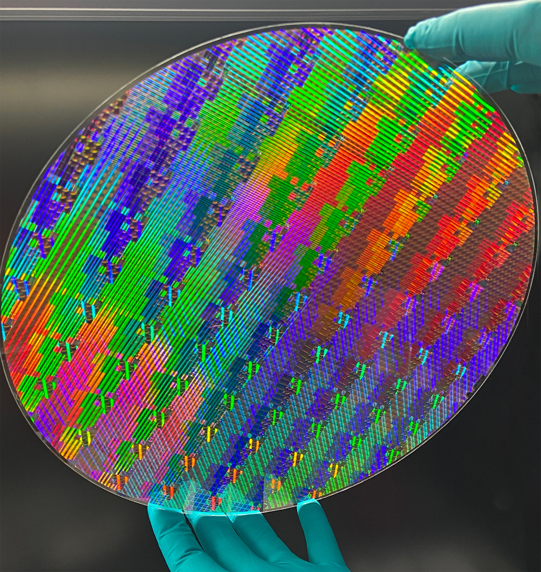
Image courtesy of Metalenz
Rob Devlin helped develop innovative mini-lens as grad student. Now the startup he runs produces millions of them for consumer electronics.
Over the course of his Harvard doctoral studies, Rob Devlin must have made 100 of a new kind of mini-lens, experimenting with materials and prototyping new designs to bend light like a traditional camera only using a series of tiny pillars on a millimeter-thin wafer.
This new device would be smaller, cheaper, and able to be mass produced — if demand ever warranted it — in semiconductor chip foundries.
Today, demand warrants it.
Metalenz, a startup founded in 2016 with exclusive rights to commercialize the device Devlin helped develop in the lab of Federico Capasso, the Robert L. Wallace Professor of Applied Physics, says some 100 million of its light-focusing metasurfaces have been made and are installed in an array of consumer electronic devices.
Metalenz — with Devlin now as CEO — wouldn’t disclose which companies are using its devices in their products, but at least one report from a company that does teardowns of consumer products, Yole Group, says metasurfaces are in the iPad, Samsung Galaxy S23 Ultra, and Google’s Pixel 8 Pro.
“It’s remarkable to think that something that started at Harvard — during my Ph.D. and with the work of all the other folks in the Capasso lab — is now out there and people are using it,” Devlin said. “There are many examples of university technology that have great promise, and having metasurfaces actually end up in real-world devices at the scale that we’re now talking about definitely has a great feel to it.”
Sam Liss, executive director of strategic partnerships at Harvard’s Office of Technology Development, said Metalenz emerged from a group that was cross-disciplinary, leveraging different scientific backgrounds and perspectives into a product that is breaking new ground.
“[Former University President] Drew Faust once said that companies create new products; university research creates new industries.”
Sam Liss, Harvard Office of Technology Development
“It’s really taking conventional optics, which have been around for a very, very long time, and disrupting that industry,” Liss said. “That’s what I think university startups are really great at: true disruption. [Former University President] Drew Faust once said that companies create new products; university research creates new industries. And that always resonated with me.”
Capasso’s early work on metasurfaces began in 2007 or 2008. By 2012, when Devlin arrived at the lab, the science was mostly figured out. In a 2011 paper in the journal Science, which has garnered more than 10,000 citations, Capasso and members of his lab showed they could tune nanostructures on the metasurface to control light at will.
Shortly after, they demonstrated the first metalens, which was able to focus light — albeit inefficiently — on a single spot. From there, Devlin added his expertise in materials and nanofabrication, working with other members of the lab to refine the product. And Capasso set the bar even higher: He wanted not only a product that worked, but one that could be mass-produced using existing fabrication methods so they could go to market quickly.
“In record time, metalenses went from a research prototype in 2016 to the creation of Metalenz in the same year and mass manufacturing for the consumer market in the following years,” Capasso said. “Kudos to Rob Devlin for successfully leading this transition.”
All along, researchers knew the device had the potential to disrupt the traditional business of making lenses from curved pieces of polished glass or plastic. As manufacturers crammed more and more features into smartphones, tablets, and other devices, it became clear that the real estate taken up by bulky lenses was a bottleneck to more advanced designs.
A major early victory for Metalenz came in 2021, when the startup signed a contract with STMicroelectronics to put its metasurfaces into STMicro’s FlightSense module.
The distance-measuring module uses near-infrared light for 3D sensing, and the metasurface is involved in both emitting light and in detecting its reflections. The time taken for the infrared light to bounce back provides key data in drawing the 3D picture. It is used in facial recognition, 3D room mapping, augmented reality, and similar applications.
Though these metasurfaces are not typically used for visual images, they can provide depth information that helps focus visual camera lenses.

Rob Devlin.
Photo courtesy of Metalenz
Metalenz is currently based in Boston’s North End and has doubled in size to about 45 employees over the last three years. The company doesn’t need all that much space, because the manufacturing is left to large semiconductor foundries, which turn out more than a trillion chips a year for the global technology industry.
At Metalenz, Devlin said, the staff focuses on improving performance of their current product and developing what they hope will be the next big breakthrough: Polar ID.
Polar ID uses polarization of light to provide an additional layer of security for smartphones with a dramatic reduction in cost and size.
Devlin said that a traditional polarization camera is about 100 millimeters long and costs $500 to $1,000. Smaller versions have been created but are found only on top-end devices. Metalenz’s polarization metasurface is about 5 millimeters long and costs roughly $5, Devlin said, which would allow their deployment at low cost in many more devices.
“I can get a standard image of you. I can recognize the distance between your eyes and how far your eyes are from your nose and all of these key landmarks,” Devlin said. “But the polarization signature of you is unique, meaning that even if someone came with a perfect 3D mask of you and put it in front of the device, the polarization signature of that 3D mask would be different than your polarization signature.”
Polarization can be used in other applications as well. For example, skin cancer’s polarization signature is different from healthy skin, so it can be used to detect dangerous growths. It can also be used to monitor air quality.
“There are a lot of exciting things stemming from the power of the metasurface to take complex modules, shrink them down, and let you do entirely new things,” Devlin said.
As with any successful product, other companies are working to catch up, Devlin said. Metalenz’s strategy is to continue to improve current products and develop new ones that leverage the technology to do new and interesting things.
He also counted among advantages their continued relationship with Capasso — a Metalenz founder — providing a pipeline to new developments from his lab.
“There’s a lot of competition and folks are trying to catch up to us,” Devlin said. “The benefit we have is really the first applications we’ve already deployed, and we’ve already started to move on to something where we’re using even more of the unique aspects of the metasurface.”