


Campus & Community
Making the world’s smallest gadgets even smaller
Harvard researchers winning race to the bottom
You may not have noticed, but the smallest revolution in world history is under way. Laboratories and factories have begun to make medical sensors and computer-chip components smaller than a single blood cell or the periods on this page.
It’s called nanotechnology. Our federal government is spending $1 billion on it this year, while corporations and investors worldwide have invested some $4 billion to date. The $13 billion in nanoproducts already on the market is expected to reach $2.6 trillion by 2014. In October, the National Cancer Institute awarded Harvard and the Massachusetts Institute of Technology (MIT) a $20 million five-year grant for applying nanotechnology to detect and treat cancer. The Harvard-MIT facility will be one of seven Centers of Cancer Nanotechnology Excellence across the country.
“Nano” stems from a Greek word meaning “dwarf,” or a billionth part of something. The standard unit in this technology is a nanometer, a billionth of a meter, a few hundreds of millionths of an inch. Atoms are about 0.2 of a nanometer across, so nanotechnologists measure sizes in atoms rather than bulky inches or millimeters.
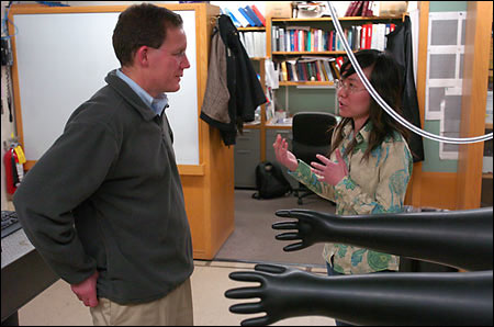
Charles Lieber, Hyman Professor of Chemistry, has been making such diminishingly small things for years. He and his colleagues at Harvard’s Department of Chemistry and Chemical Biology and the Division of Engineering and Applied Sciences have fabricated detectors for viruses and prostate cancer that measure about 10 nanometers (50 atoms) in size. (Visit http://www.hno.harvard.edu/gazette/2005/09.29/11-cancer.html.)
The race to the bottom of matter involves not only constructing smaller, more efficient devices but also finding better ways to make the tools needed to produce these things. In the November 25 issue of the journal Science, Lieber, along with graduate students Chen Yang and Zhaohui Zhong, announced a unique way to fabricate nanodevices. Instead of using conventional methods to make wires that connect together nanotransistors and other circuit components, this team built the components right into the wires. Rather than constructing a device that is later programmed to contain information and to perform a function, they built the information and function right into the wires.
Here’s the way Lieber puts it: “We have demonstrated the controlled synthesis of nanostructures at levels of complexity significantly beyond any work yet reported. What we have done is the most challenging synthetic problem in these structures, and one with huge potential payoffs from both the standpoint of fundamental scientific impact and producing novel devices and applications.”
Pushing limits
Nanostructures are now produced using complex, expensive, lithographic techniques. If you want to make a computer chip with switches and other devices connected by wires, you first make a pattern of the circuits. This pattern is laid over silicon or another material then exposed to an etching medium. Chemicals, light, or beams of particles “carve” out spaces not covered by the pattern. Some sort of metal fills the etched spaces, producing a circuit printed into a semiconducting material like silicon.
Such lithography production lines now cost in excess of $1 billion. Lieber’s technique would provide nanodevices that can run everything from toys, to medical probes, to supercomputer chips without lithography. These devices would not only be cheaper but would provide more efficiency.
Lithography has it limits. You can’t make anything smaller than the spaces on the pattern. In other words, there are limits to how many devices you can put on a computer chip. Intel Corp., the world’s leading chipmaker, has squeezed more than 1 billion switches on a chip the size of a thumbnail. That’s why children now play with toys that boast more computing power than the spacecraft that landed two men on the moon in 1969.
Today, Intel will sell you a fully functioning memory chip with switches that measure a meager 35 nanometers across. But eventually these devices get so close to each other that heat and electric fields generated by the crowding could render the circuits inoperable.
In their report in Science, Lieber and his colleagues announced that they found the way to solve such problems and move ahead in the race to the smallest. “We can push to 3-5 nanometers (roughly 15 to 25 atoms), which will not be possible to achieve with lithography,” they say.
This lithography-less technology builds switches, amplifiers, and other devices right into silicon nanowires, as they are made. Wires sit in a vacuum in a reactor in which different gases precisely flow onto sharply defined sections. The gases add impurities to the silicon, a process called doping. The amounts and types of dopants change the charges within, and the electrical conductivity of the wires, switching electricity or light on or off, amplifying them, or changing them in other ways.
Such doping-sequenced nanowires are now made only in laboratories on the Harvard campus, but Lieber says, “We don’t see any problems with scaling up to factory production.”
The nanofuture
Doped nanowires promise smaller, faster, and cheaper electronic and photonic (light-carrying) devices for the future. But more than that, by demonstrating the concept of encoding information and function during synthesis, “we show a fundamentally new approach to building complex things,” Lieber notes.
The possible uses and impact of doped nanowires seem only limited by imagination. Lieber’s lab has already constructed a nanogadget by lithography that has the potential to detect and distinguish between single viruses. Such a detector would come in handy now that the world is on a nervous lookout for Asian bird flu.
Viruses are among the most important causes of human diseases and are of increasing concern as agents of bioterrorism. Nanoscale silicon wires could be fashioned into chip arrays capable of sensing thousands of different viruses, ushering in a new era for quick response to viral outbreaks.
Lieber and his colleagues have also built a cracker-size detector for cancer. Someday, such sensors might be used to test people for cancers in doctors’ offices.
Other potential nanodevices being looked at may help doctors detect whether cancer has spread, or is shrinking in response to treatments. In the future, nanoparticles might travel through human bodies and deliver cargoes of drugs to malignant tumors, eliminating the need for surgery or greatly reducing the side effects of chemotherapy.
And no one doubts that nanodevices and techniques will make possible many types of smaller, faster computers, medical instruments, and personal gadgets that bring increased convenience and pleasure.
“I think no virtue goes with size.”
– Emerson