
Campus & Community
Harvard wins nanocenter grant
A group of faculty at Harvard, the Massachusetts Institute of Technology (M.I.T.), and the University of California, Santa Barbara, is one of a handful nationwide to win millions of dollars in National Science Foundation funding to begin a Nanoscale Science and Engineering Center – which will explore and manipulate items as small as a single atom.
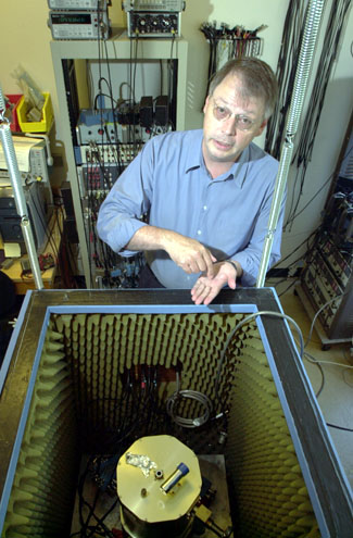
Robert Westervelt, Gordon McKay Professor of Applied Physics and Professor of Physics, said the presence of Harvard’s Center for Imaging and Mesoscale Systems (CIMS), which has facilities and equipment available to conduct nanoscale research (such as a “clean room” and electron microscopes), was a big factor in winning the grant.
Nanotechnology is one of sciences’ new frontiers. It is already used to manufacture things ranging from military combat suits to scratch-proof eyeglasses to additives for plastic. In addition, the technology promises things such as computer chips with parts approaching the size of atoms.
Westervelt said he was very pleased to win the $10.8 million grant and said one of its main features is that it will aid collaborations between its universities and research labs.
Harvard’s partners in the center include the M.I.T., the University of California, Santa Barbara, the Delft University of Technology, the University of Tokyo, and the National Laboratories at Brookhaven, Oak Ridge, and Sandia.
“The point is to promote collaborations among investigators who work in different fields and whose work requires input from people in different fields,” Westervelt said. “We will have an active travel program to allow students to travel.”
The center begins operations this month with Westervelt as principal investigator and director; CIMS director and Hollis Professor of Mathematics and Natural Philosophy Bertrand I. Halperin as co-principal investigator; several dedicated staffers, including an associate director and technical staff. The grant runs for five years and can be renewed for a second five-year period.
In addition to promoting the development of technology, the grant’s purpose is to develop and establish a work force skilled in nanotechnology.
“With its nanoscale science and engineering initiative, the National Science Foundation [NSF] is enabling the coming wave of research,” said Mihail Roco, head of the NSF initiative and chair of the National Science and Technology Council’s subcommittee on Nanoscale Science, Engineering and Technology. “Each of the six centers has a bold vision for research at the frontiers of science and technology, and together they will provide coherence and a longer-term outlook to U.S. nanotechnology research and education.”
Along with its research and academic features, the new Nanoscale Science and Engineering Center will have a public outreach component. Westervelt said it will work with the Museum of Science in Boston to create workshops on nanotechnology for the public. It will also sponsor educational workshops for Cambridge and Boston public school students and their teachers.
In addition to using the CIMS facilities, Westervelt said the new center’s federal funding will enable it to enhance them, by adding new equipment and staff dedicated to the new center.
“The two [CIMS and the new center] are tied together in important ways,” Westervelt said.
The new center’s work will combine two approaches to building things on an extremely tiny scale. The first is what Westervelt called a “top-down” approach, used in techniques such as electron-beam lithography where an electron stream is used to etch a pattern on a semiconductor. The second, which Westervelt referred to as “bottom-up,” is where chemical techniques build an item up from individual atoms.
Each technique has its drawbacks, he said. The “top-down” approach has limits in how small it can go. The “bottom-up” technique creates very small items. It is very difficult using that technique, however, to assemble the items into useful structures, he said.
Other potential developments would be a new type of computer memory, using very tiny, high-density magnetic particles or new kinds of computer circuitry using individual electrons whose spin can be controlled and switched at will.
Westervelt said part of the interest with nanoscale devices is that they’re so tiny that they’re on the border between the everyday world and the world of quantum mechanics – where particles can be in several places at once.
“The devices get so small that the quantum effects you usually only see in someone’s lab will be in a product that is coming out,” Westervelt said. “This will require new techniques and no one is sure what they will be.”