

Science & Tech
Applied physicists create building blocks for a new class of optical circuits
Devices exhibit customizable optical properties suitable for wide range of applications
Imagine creating novel devices with
amazing and exotic optical properties not found in nature — by simply
evaporating a droplet of particles on a surface.
By chemically building clusters of nanospheres from a liquid, a team of
Harvard researchers, in collaboration with scientists at Rice
University, the University of Texas at Austin, and the University of
Houston, has developed just that.
The finding, published in the latest issue of Science, demonstrates
simple scalable devices that exhibit customizable optical properties
suitable for applications ranging from highly sensitive sensors and
detectors to invisibility cloaks.
Using particles consisting of concentric metallic and insulating shells,
Jonathan Fan, a graduate student at the Harvard School of Engineering
and Applied Sciences (SEAS), his lead co-author Federico Capasso, Robert
L. Wallace Professor of Applied Physics and Vinton Hayes Senior Research
Fellow in Electrical Engineering at SEAS, and Vinothan Manoharan,
associate professor of chemical engineering and physics in SEAS and
Harvard’s Physics department, devised a bottom-up, self-assembly
approach to meet the design challenge.
“A longstanding challenge in optical engineering has been to find ways
to make structures of size much smaller than the wavelength that exhibit
desired and interesting properties,” says Fan. “At visible frequencies,
these structures must be nanoscale.”
In contrast, most nanoscale devices are fabricated using top-down
approaches, akin to how computer chips are manufactured. The smallest
sizes that can be realized by such techniques are severely constrained
by the intrinsic limits of the fabrication process, such as the
wavelength of light used in the process. Moreover, such methods are
restricted to planar geometries, are expensive, and require intense
infrastructure such as cleanrooms.
“With our bottom-up approach, we mimic the way nature creates innovative
structures, which exhibit extremely useful properties,” explains
Capasso. “Our nanoclusters behave as tiny optical circuits and could be
the basis of new technology such as detectors of single molecules,
efficient and biologically compatible probes in cancer therapeutics, and
optical tweezers to manipulate and sort out nano-sized particles.
Moreover, the fabrication process is much simpler and cheaper to carry
out.”
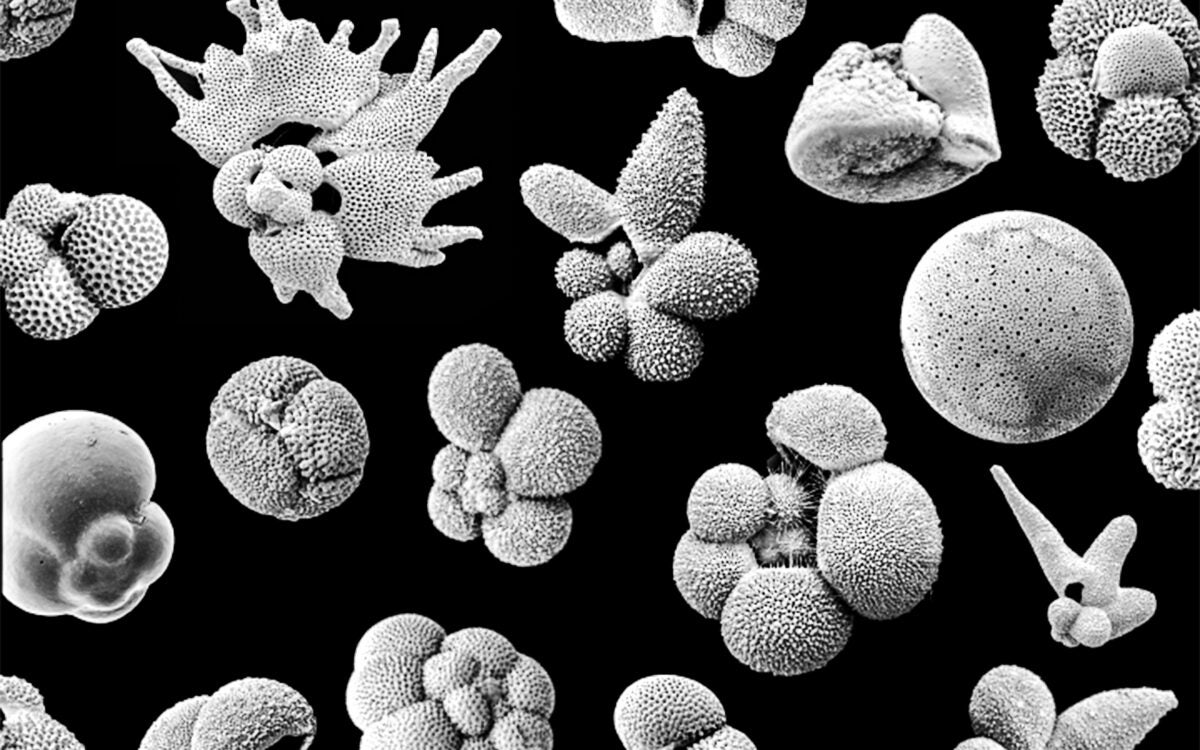
The researchers’ self-assembly method requires nothing more than a bit
of mixing and drying. To form the clusters, the particles are first
coated with a polymer, and a droplet of them is then evaporated on a
water-repellent surface. In the process of evaporation, the particles
pack together into small clusters. Using polymer spacers to separate the
nanoparticles, the researchers were able to controllably achieve a two
nanometer gap between the particles — far better resolution than
traditional top-down methods allow.
Two types of resulting optical circuits are of considerable interest. A
trimer, comprising three equally-spaced particles, can support a
magnetic response, an essential property of invisibility cloaks and
materials that exhibit negative refractive index.
“In essence, the trimer acts as a nanoscale resonator that can support a
circulating loop of current at visible and near-infrared frequencies,”
says Fan. “This structure functions as a nanoscale magnet at optical
frequencies, something that natural materials cannot do.”
Heptamers, or packed seven particle structures, exhibit almost no
scattering for a narrow range of well-defined colors or wavelengths when
illuminated with white light. These sharp dips, known as Fano
resonances, arise from the interference of two modes of electron
oscillations, a “bright” mode and a non-optically active “dark” mode, in
the nanoparticle.
“Heptamers are very efficient at creating extremely intense electric
fields localized in nanometer-size regions where molecules and nanoscale
particles can be trapped, manipulated, and detected. Molecular sensing
would rely on detecting shifts in the narrow spectra dips,” says Capasso.
Ultimately, all of the self-assembled circuit designs can be readily
tuned by varying the geometry, how the particles are separated, and the
chemical environment. In short, the new method allows a “tool kit” for
manipulating “artificial molecules” in such a way to create optical
properties at will, a feature the researchers expect is broadly
generalizable to a host of other characteristics.
Looking ahead, the researchers plan to work on achieving higher cluster
yields and hope to assemble three-dimensional structures at the
macroscale, a “holy grail” of materials science.
“We are excited by the potentially scalability of the method,” says
Manoharan. “Spheres are the easiest shapes to assemble as they can be
readily packed together. While we only demonstrated here planar particle
clusters, our method can be extended to three-dimensional structures,
something that a top-down approach would have difficulty doing.”
Fan, Capasso, and Manoharan’s co-authors included Chihhui Wu and Gennady
Shvets of University of Texas at Austin; Jiming Bao of the University of
Houston; and Kui Bao, Rizia Bardhan, Naomi Halas, and Peter Norlander,
all of Rice University.
The researchers was supported by the National Science Foundation;
the Air Force Office of Scientific Research; the U.S. Department of
Defense; the Robert A. Welch Foundation; and the Center for Advanced
Solar Photophysics, a U.S. Department of Energy Frontier Research
Center. The work was carried out at the Center for Nanoscale Systems at
Harvard, a member of the National Nanotechnology Infrastructure Network.